 Image: Gordon Mah Ung
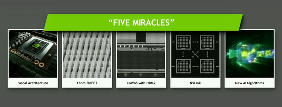
“At Nvidia, we have a rule. No project should ever rely on three miracles,” CEO Jen-Hsun Huang said, pacing the stage during Tuesday’s GTC conference in San Jose, California. “The Tesla P100 has five miracles.”
And indeed, Nvidia’s monstrous new graphics module for hyperscale datacenters seems downright heavenly, with more than twice as many transistors as the company’s current-gen Maxwell GPUs. While the lack of news about consumer graphics cards at GTC was a bit disappointing, the first product packing the big-boy Pascal graphics looks so darn fantastic that the sting wore off in seconds.
The Tesla P100 packs numerous cutting-edge technologies, from 16nm FinFET transistors—after graphics processors spent four long years stuck on the 28nm node—to second-generation high-bandwidth memory (HBM) technology to Nvidia’s own Pascal GPU architecture to Nvidia’s blazing-fast NVLink interconnect technology. These features constitute four of the miracles, and they all serve to support the fifth: advanced AI learning algorithms.
“So many new pieces of tech had to happen for this,” Huang beamed.

The Pascal GPU at the heart of the Tesla P100, which Nvidia’s been teasing for two years now, takes advantage of the long-delayed transition to 16nm transistor technology, with a whopping 15 billion transistors crammed into a 600 millimeter square chip. “If I held it up right now you could see it from the back row,” Huang joked.
That’s more than twice as many transistors as the 7 billion found in Maxwell, and the Tesla P100 cranks through 5.3 teraflops of double-precision floating-point performance and 10.6 teraflops of single-precision performance. By comparison, the Titan X offers 7 TFLOPS of single-precision floating-point performance.
Update: After the keynote ended, Nvidia published full Pascal GPU architecture information, complete with speeds, feeds, and block diagrams. Check out PCWorld’s Pascal GPU tech deep dive for the full scoop.
That 600mm die size (assuming that’s the die size, and doesn’t include other parts) likely didn’t happen by accident; AMD’s high-end Fiji chips measure in at 596mm squared. The Tesla P100 takes another page from the Fiji playbook with the inclusion of 16GB of lightning-fast second-gen HBM memory, after the technology made its debut in the Radeon Fury X. Whereas high-end Nvidia Maxwell GPUs connect to memory via a bus of 384 wires, Huang says that the Tesla P100’s memory and GPU communicate over a whopping 4,000 wires. Overall, the module features more than 15 billion transistors in total. That’s nuts.

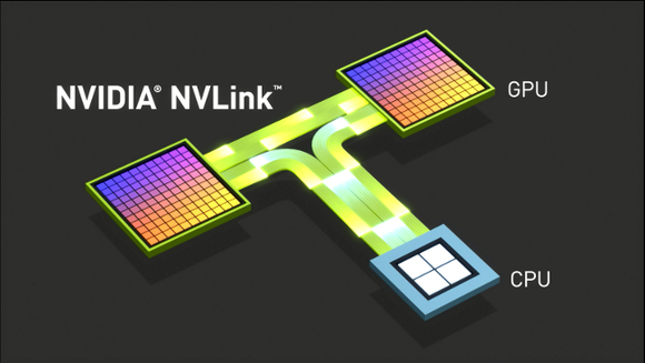
But the new tech doesn’t stop there! The Tesla P100 features Nvidia’s new NVLink interconnect technology, which allows graphics modules to communicate with each other and CPUs at five times the aggregate bi-directional speed of a standard PCIe connection. Plus, it lets you bring more friends to the graphical computing party, supporting up to eight GPU connections rather than PCIe’s four.
Last year, Huang teased that systems packing Pascal graphics would wind up being 10 times faster than Maxwell-based systems. The reality wound up being even more lofty, he says. When you take into account NVLink, Pascal optimizations, HBM2, and the sheer number of transistors on the chip, Huang says that you’ll actually see a 12-fold increase in speed, citing a workload that completes in 25 hours on a Maxwell PC, but just two on a Pascal system.

Miraculous indeed. The Nvidia Tesla P100 is in volume production today and will wind up in server products in the first quarter of 2017, likely due to HBM constraints.
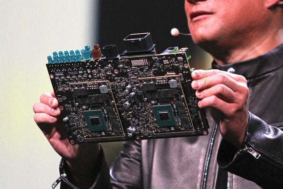
Expect to see all that juicy new GPU tech dribble down to consumer graphics cards sometime in the coming months, too. We may have gotten our first glimpse of it on the back of Nvidia’s Drive PX2 board for smart vehicles, which featured a pair of what Huang said were unannounced GPUs.
 Gordon Mah Ung
Is that our first look at a more modest Pascal GPU chip that may wind up in consumer graphics cards? In any case, a quick glance at the graphics chips (you can click the image to enlarge it) show them surrounded by traditional memory chips, rather than HBM modules—so not all Pascal-powered GPUs will ditch GDDR5 RAM. Hint, hint.


